
| HS Code | 663216 |
| Material Type | Organic |
| Emission Color | Variable (Red, Green, Blue, etc.) |
| Carrier Mobility | Typically 10^-6 to 10^-4 cm2/Vs |
| Glass Transition Temperature | Usually 80-150°C |
| Quantum Efficiency | Up to 100% (phosphorescent materials) |
| Work Function | Approximately 5.0-6.0 eV |
| Thermal Stability | Moderate to High |
| Film Formability | Excellent |
| Lifetime | Up to 100,000 hours (for some materials) |
| Solubility | Soluble in organic solvents |
| Charge Transport | Electron and hole transport capability |
| Decomposition Temperature | 200-500°C |
| Purity Requirement | Above 99.99% |
| Photostability | Moderate |
| Environmental Sensitivity | Sensitive to oxygen and moisture |
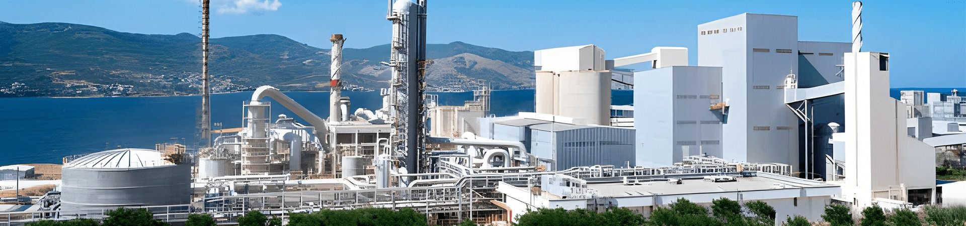
As an accredited OLED Materials factory, we enforce strict quality protocols—every batch undergoes rigorous testing to ensure consistent efficacy and safety standards.
| Packing | The OLED Materials are securely packaged in a 100-gram amber glass bottle with tamper-evident seal, labeled for safe handling. |
| Container Loading (20′ FCL) | 20′ FCL container for OLED Materials typically holds 10-12 tons, securely packed in drums or fiber cartons, ensuring safe, moisture-free transit. |
| Shipping | OLED materials are shipped in tightly sealed, moisture-resistant containers to protect against air and light exposure. Packaging complies with relevant hazardous materials regulations, ensuring safe transport. Temperature controls and handling instructions are included to maintain material integrity during transit. Proper labeling and documentation accompany all shipments for regulatory and safety compliance. |
| Storage | OLED materials should be stored in tightly sealed containers, away from light, moisture, and air to prevent degradation. Store in a cool, dry, and well-ventilated area, typically in a glovebox or environment with inert gas such as nitrogen or argon. Ensure materials are clearly labeled, and avoid exposure to elevated temperatures or direct sunlight. Handle with appropriate personal protective equipment. |
| Shelf Life | The shelf life of OLED materials typically ranges from 1 to 3 years when stored in cool, dry, and inert conditions. |
As a direct manufacturer specializing in OLED materials, we supply high-performance chemicals tailored for advanced optoelectronic industries. Our products address the specific requirements of major downstream sectors, integrating directly into complex fabrication environments. The following application areas reflect practical industrial adoption and regulatory adherence for OLED chemicals, from prototyping to high-throughput mass production.
We supply OLED emitter, host, and transport layer materials for active-matrix organic light-emitting diode (AMOLED) panel lines. Our materials undergo stringent QC suited for vacuum thermal evaporation and inkjet printing. They enter panel production at the EL device layer deposition stage, ensuring reproducible light output and defined color coordinates. Downstream customers adjust blend ratios for blue, green, and red stacks, impacting luminance and device life. Panel manufacturers reference our lot-to-lot traceability and recalibrate process settings for yield stability.
Industry compliance standards
Typical usage ratio
Downstream process integration
Final product types
We manufacture high-purity emission materials and charge transport chemicals for solid-state lighting panels. These meet lighting fixture specifications for white and tunable color output. Lighting companies depend on our OLED molecules for stable quantum yield and suppression of voltage drift under continuous operation. White light panels require precise mixing of blue, green, and red emitters plus broad-spectrum host layers. Our product batches support various roll-to-roll and sheet manufacturing workflows, including encapsulation and in-line patterning.
Industry compliance standards
Typical usage ratio
Downstream process integration
Final product types
Our specialty OLED chemicals match the precision and resolution standards essential for microdisplay fabs supplying augmented reality and near-to-eye devices. These lines require sub-micron control of emitter and electron/hole transport molecular layers. Diagnostics during processing depend on our certified material purity, reducing defect rates and guaranteeing targeted train size emission. We maintain consistent energy level alignment for device miniaturization needs.
Industry compliance standards
Typical usage ratio
Downstream process integration
Final product types
For high-definition display and signage applications, our OLED materials support photolithographic patterning. This process requires specialized cross-linkable or photoactive small molecules and polymers tailored for solvent and UV exposure during pixel definition. We deliver materials with tight molecular weight distributions and low ionic residue, preventing contamination or refractive index deviation. Photo-patternable layers permit thin-film transistor (TFT) backplane alignment and high-resolution RGB subpixel formation for advanced signage.
Industry compliance standards
Typical usage ratio
Downstream process integration
Final product types
Competitive OLED Materials prices that fit your budget—flexible terms and customized quotes for every order.
For samples, pricing, or more information, please contact us at +8618018036652 or mail to sales6@ascent-chem.com.
We will respond to you as soon as possible.
Tel: +8618018036652
Email: sales6@ascent-chem.com
Flexible payment, competitive price, premium service - Inquire now!
Organic Light Emitting Diode materials have steadily grown from a handful of research vials on our benches to ton-scale production in our reactors. Our journey with OLED materials runs deep, marked by small breakthroughs and constant adaptation alongside display manufacturers. Early panels flickered with uneven color or issues in blue light output. Now, sharpness and color depth impress across mobile phones, TVs, and wearables. Having worked closely with OLED developers for over a decade, we approach the topic from lived experience—balancing consistent chemical processing with continuous invention.
OLED materials are not like bulk commodity chemicals made by the railcar. Achieving the slightest improvement in quantum efficiency or stability often means tweaks at the molecular level. Our batches rarely stretch beyond a few hundred kilograms, and each production run presents its own puzzles—whether it’s a tricky purification step or meeting the sparse tolerances on metal contaminants demanded by thin-film deposition. This work demands an understanding of what actually happens during device fabrication and a willingness to adjust synthesis procedures based on downstream feedback.
One example comes from the synthesis of blue emissive layers. Unlike green or red emitters, blue molecules need to minimize triplet excitons to avoid efficiency losses, requiring us to control the molecular weight distribution and ensure a certain glass transition temperature. During mass production, scaling up a reaction while suppressing side products means more than just adding larger reactors and thicker jackets; it involves precise catalyst and temperature controls under an inert atmosphere. We’ve invested in specific distillation units and implemented in-line analysis—pulling product samples mid-run—to identify off-spec batches instantly.
Pure, single-component emitter models such as our 5,5'-bis[N-(1-naphthyl)-N-phenyl]benzidine (NPB) highlight the difference between laboratory curiosity and plant-scale output. For an emitter like tris(8-hydroxyquinolinato)aluminum (Alq3), color purity hinges on trace metals and particle size. Device engineers want predictable emission and a narrow energy gap, and even minor off-target impurities show up in the finished product as lower brightness or unexpected color drift over time.
Our R&D group regularly collaborates with film-formers in the next building to match vapor pressure and purity requirements for sources like 4,4'-bis(carbazol-9-yl)biphenyl (CBP) matrices. Rather than treat the host, emitter, and dopant as a simple recipe, we tailor each batch for a cohesive, high-yield process. Customers testing our batches in actual devices uncover subtleties no analytical assay detects—like how a ten-parts-per-million change in halide content creates micro-bubbles during thermal evaporation.
Display makers no longer tolerate high drift or short lifespans in their device stack, and neither do we. For an OLED material to earn a place in a flagship screen, its stability under high current and strong light cannot just meet an internal metric; it must show consistent results across several cycles and in real-world applications. We track every lot’s volatility and residual solvent profiles, running thermal gravimetric analysis and comparing it with the last three production runs to flag deviations that could lead to shorter panel lifespans.
Oxidative degradation stands as a major hurdle. Many emitter molecules react with trace oxygen during storage or within the device itself. Where we used to rely on large-scale vacuum ovens, we’ve since gone over to sealed manufacturing lines and redundant gas purging. This move required investment in both equipment and training but yielded a cleaner, more reliable emitter—confirmed by materials that retain intensity after thousands of hours under harsh conditions.
OLED chemicals distinguish themselves from older inorganic light-emitting display materials on more than just cost. Traditional display backlights use rare earth phosphors like YAG:Ce or QD nanoparticles, which focus output through an excited, lattice-bound state. In OLEDs, the emission occurs from organic layers governed by molecular design and thin-film morphology. This quality allows for more flexibility in color tuning but introduces stricter demands for purity and batch-to-batch sameness.
Some competitors offer rare earth or non-OLED phosphors in bulk, but these do not enable the ultra-thin, flexible form factors sought by consumer device brands. Our customers claim the major performance gap shows up in contrast, response time, and the ability to manufacture bendable and transparent panels. Few display makers can risk switching to OLEDs without a tight partnership upstream—one that prioritizes reliable synthesis and logistical agility.
The emphasis on material performance in clinical literature or news reports rarely covers what manufacturers face scaling production from grams to kilograms. For instance, an emitter optimized in the lab might degrade rapidly under scaled-up purification or show strong aroma and volatility, causing safety or yield issues that simple simulation overlooks. We’ve solved such problems using staged distillation, real-time gas-phase detection, and personalized training for each staff group handling sensitive intermediates.
Batch processes expose more opportunities for environmental control and in situ intervention compared to continuous-flow reactors used elsewhere in fine chemicals. As a manufacturer, we favor small-lot, closely monitored runs for these specialty compounds. For every new model adopted by a big display maker, we double down on sample archiving and failure mode analysis. Should a customer report a slight discoloration after month-long aging, we can trace the lot, test retained samples, and adjust parameters to guarantee the issue disappears by the next run.
Sustainability in the OLED world cannot be tacked on at the end of the process. Our commitment starts with greener precursors and safer solvents. Pressure from both regulatory changes and multinational clients has pushed us to design routes that minimize halogenated byproducts, lower solvent footprints, and capture reaction off-gasses for reprocessing. There is no silver bullet, but by optimizing yields and recycling internal waste streams, we see reduced costs and sharper quality benchmarks.
Some of our most successful process changes came from operators not content to leave well enough alone. Switching to a recycled solvent loop—once doubted by half our team—reduced emissions by over thirty percent without impacting product purity. We publish our process energy metrics for each OLED material grade, providing evidence to both customers and our own teams about areas for further improvement. Each step towards greener chemistry comes back to the experience and knowledge built on the ground, not in conference rooms or analyst briefs.
No automated system or software program replaces the intuition of a well-trained chemist or technician at the production line. Making OLED materials at high consistency involves recognizing subtle cues—a color change in a distillation column, a shift in UV-vis output that means something went off-script. We continually run in-house workshops to keep both experienced and new staff alert to these signs, building a deeply rooted skill set rarely found outside experienced specialty chemical manufacturing.
We encourage chemists to question historical assumptions and communicate openly with device engineers and QA teams. Through regular feedback cycles, staff across synthesis, analysis, and customer application labs swap notes, which helps us catch issues before they leave the factory floor. An example from earlier this year: A reactor operator spotted an early-stage haze pointed out by a technician as a threat for device yield issues, confirming the value of hands-on experience despite advances in process digitalization.
The OLED industry evolves rapidly; one month a customer wants high color purity for a flagship TV application, the next they shift focus to materials suitable for flexible, foldable screens in wearables. Over the past several years, our product range has expanded to meet requests for both classic, proven models—like doped phosphorescent emitters and host materials for blue and green EML—and more advanced TADF (thermally activated delayed fluorescence) molecules.
We produce across three major categories: small molecule dopants, ubiquitous host compounds, and specialty electron-transport or hole-transport layers. For each, customers want consistent thermal characteristics, high charge carrier mobility, and minimal cross-talk between layers. Some OLED models use layers as thin as 15 nm; contamination here can mean visible pixel defects at the consumer level. Finding small, deliberate modifications to synthetic routes that promote both device performance and chemical safety sets us apart from batch resellers who move products without tracing performance downstream.
Recent interest in quantum dots and hybrid organic-inorganic systems has challenged our R&D team to develop compatible interfaces. We partner closely with equipment makers to confirm our OLED chemical models fit varied vacuum deposition techniques—whether thermal evaporation, inkjet printing, or slot-die coating.
Larger display customers expect continuous supply and strict traceability for every OLED materials batch. Smaller startups building on laboratory innovation crave custom molecular tweaks, fast feedback, and small-lot flexibility. We bridge these demands with a modular production schedule and in-house analytical capabilities. Our hands-on knowledge from years in the field gives our customers more than just a bottle of chemicals; we serve as their materials troubleshooting partner, delivering testing data, technical advice, and improvement recommendations upon request.
A strong supplier-customer relationship based on transparent collaboration and consistent follow-through brings innovation to market faster and with fewer device failures. Beyond just delivering order fulfillment, we stay involved after every batch, reviewing field test results, and adapting processes to support both yield and creativity. Building trust through traceable, repeatable manufacturing practices makes the difference in long-term partnerships.
When an OLED panel passes millions of cycles without losing brightness, reminds us why our commitment to detail and precision matters. Trusted brands can risk their reputation on panels that hold color accuracy and sharpness through months of continuous use. Materials with subpar batch consistency, excess moisture, or trace degradation products all translate to premature pixel aging or even device failure. We run full lifecycle stress tests on every model, closely logging the correlation between chemical process variation and final device outcome.
Investment in high-resolution analytics, such as frontier NMR, GC-MS, and trace ionic impurity detectors, ensures that we speak with certainty about every bottle we produce. We encourage client engineers to audit our facilities, review our test data, and validate each new OLED material grade in their own workflows. By keeping our process open for discussion and improvement, we strengthen both our materials portfolio and industry reliability as a whole.
As the OLED industry matures, customers demand not just improved emission efficiency but new features—flexibility, transparency, and lower-power operation. For manufacturers like us, success means responding quickly to application feedback, retraining teams, and investing in more precise and responsive analytical tools. The next wave of chemical innovation will likely come from more sustainable chemistry, increased device longevity, and the marriage of organic emitters with novel encapsulation materials.
Day-in, day-out manufacturing of OLED chemicals may look routine, but every batch sets the stage for the displays consumers admire in homes, cars, and offices worldwide. Grounding that work in decades of accumulated experience, active process innovation, and close collaboration with device developers keeps our process rooted in value. As new generations of displays emerge, our ongoing investment in both technology and relationships places us on the front line of turning chemistry into visible impact.